Electrocardiogram PCB
Created a four-layer mixed-signal PCB for measuring biopotentials across four channels with 24-bit resolution.
February 2026
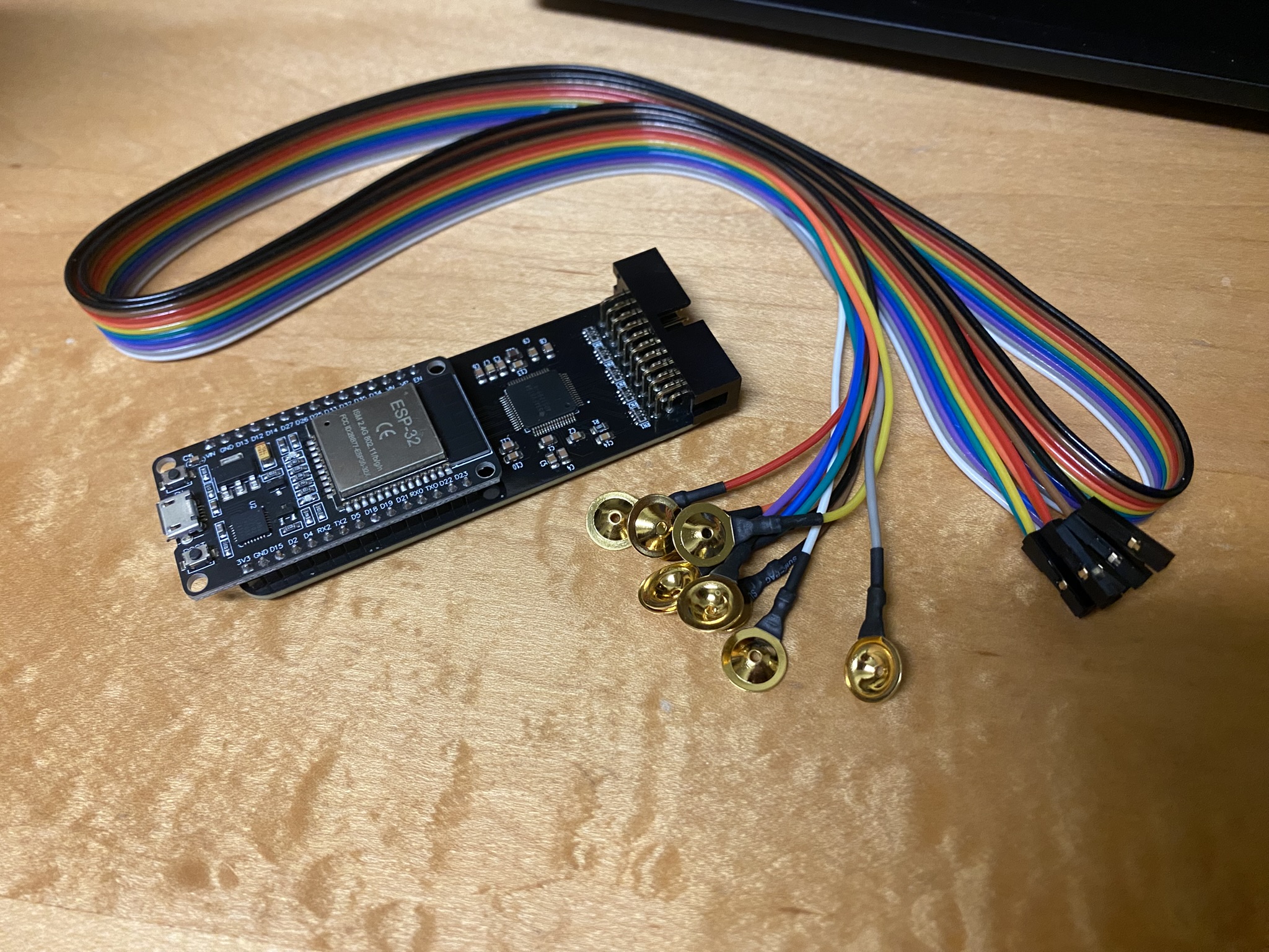
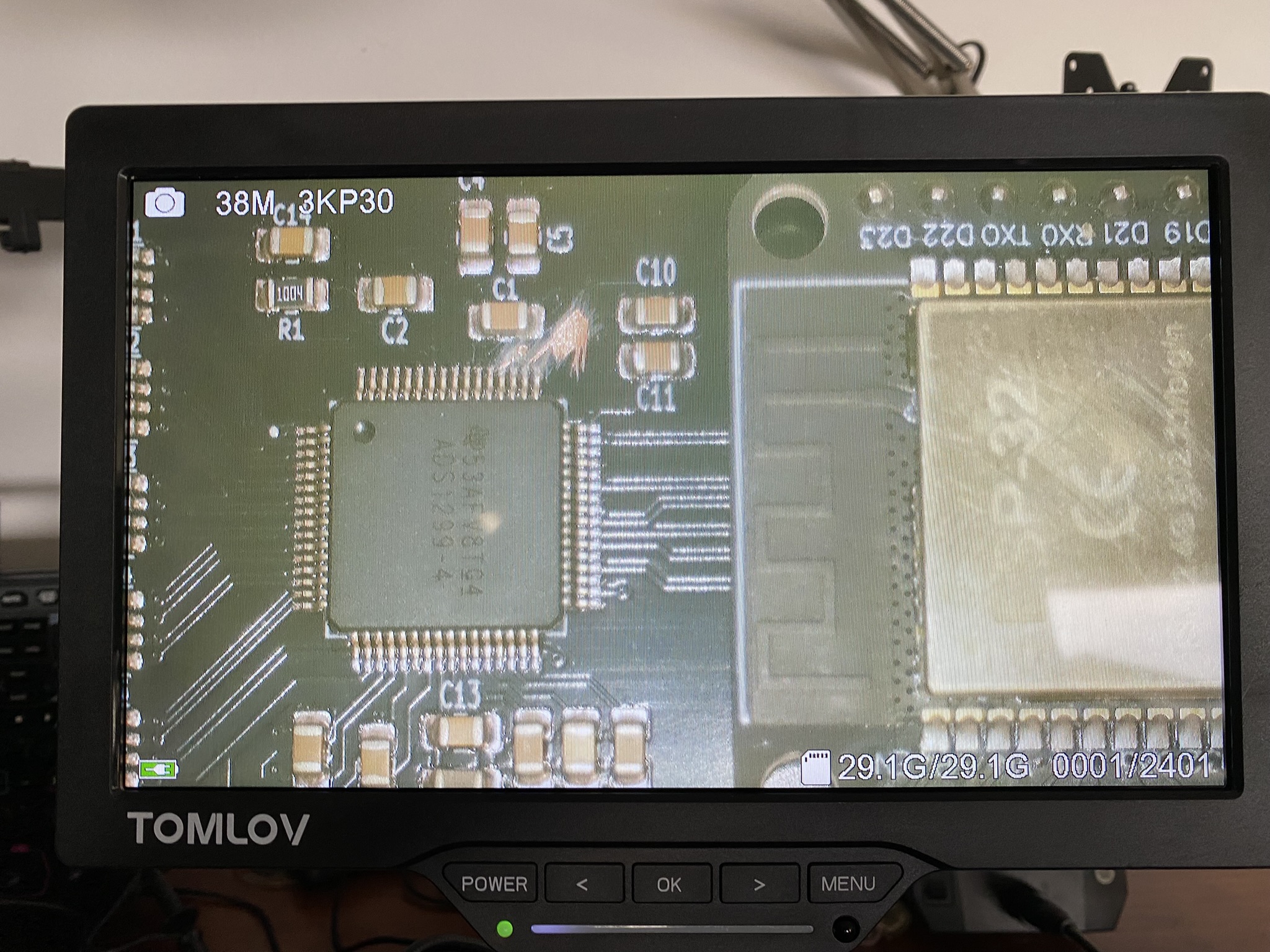
I designed a four-layer circuit board for measuring biopotential. The project was mainly centered around this Texas Instruments analog-to-digital converter. I tried to maximize SNR in my choice of regulators and my approach to layout. I also implemented a simple passive butterworth filter on each channel input to prevent aliasing.
I made the fatal mistake of routing +2.5 V AVDD power supply to a +3.3 V DVDD pin used for clock select. As a result, the board does not use its built-in internal oscillator and expects a non-existent external clock, rendering it useless. This serves as a useful lesson that I should be more careful in reviewing my layout for errors.
The opportunity to process and analyze the signals extracted from the sensor is the real highlight of this project for me, maybe even perform pattern recognition with machine learning models. The design of the PCB afforded me the opportunity to apply my EE knowledge while buliding something relatively inexpensive for some other purpose.
I may revisit this project in the future. I have ideas for separating the analog and digital ground planes, adding additional filters on regulator outputs to improve SNR, and potentially embedding the microcontroller to the board (which I decided against for simplicity).
month year
Placeholder text